Hi,
I would like to understand what CCD area you think will be usable for processing.
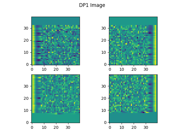
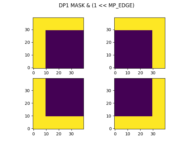
In the DP1 images, it appears that a 10-pixel boundary has the MP_EDGE mask bit set. Does this mask bit mean that these pixels are omitted from coadds, measurements, fitting, etc? Or is this just an “informational” mask?
Here is my (ahem) beautiful plot of the MASK extension corners:
Thank you,
dustin